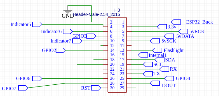
Modular Board Design Allows future support of other LoRA Micro-controllers. The initial design is around the HelTec V3 – a well supported Meshtastic LoRA Microcontroller.
The diagram below depicts how a supported LoRA equipped micro-controller (HelTec v3) plugs into a ‘Carrier Board’ which routes selected GPIO pins to a 2×15 header arrangement. I plan to ‘open-source’ the Carrier Board and would appreciate input from the Meshtastic community.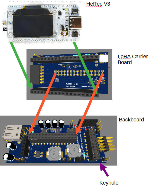
The LoRA Carrier Board maps ‘unused’ GPIO pins to the ‘back board’. The diagram (v 0.1) depicts a HelTec V3 with pins that I selected. This modular design will allow future support for other LoRA boards. This design utilizes a SDA/SCL (I2C) (using HelTec GPIO 47/48 respectively) and UART RX/TX (HelTec RXD (pin 5) and TXD (pin 6) both of which are passed through to the ‘keyhole’ at 3.3 logic levels. GPIO pins 2,3,4,6,7 are passed to the ‘backboard’ and GPIO pins 4,6,7 are passed directly to the keyhole.
GPIO 6 can be used as an alternate ‘DATA’ line (DOUT) to the daisy-chain.